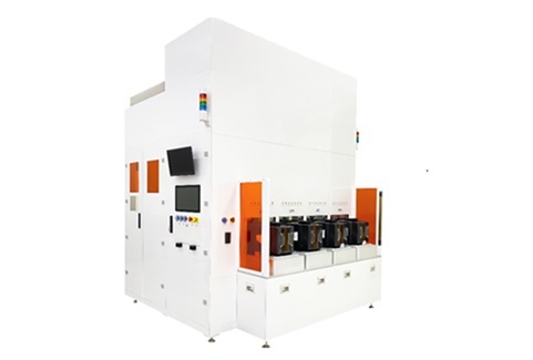
Grail B1203A Wafer Transfer System
Advantages
Strong compatibility
Multiple transmission methods
Multiple modes
Crane system interaction
Innovation
Multiple loading and unloading modes
High cleanliness level
Multiple functional options
High production capacity
International Certification
Application areas
Semiconductor Integrated Circuit
Semiconductor—Advanced Packaging
Power semiconductor
Compound semiconductor
| Low Particulate Generation | PA add≤5ea@28nm |
| High Reliability | Failure Rate ≤50 ppm |
| High Capacity | WPH≥700 |
| Dual Process Paths | Realization of independent path distinction before and after single-channel process |
| Scanning | Real-time Mapping throughout the entire process, Lot information data comparison |
| Close-fitting Method | Double 25 Batch |
| Defect Identification | Wafer interaction anomaly detection |
Related Products
 wafer cassette transport and storage system")

300mm (nitrogen) wafer cassette transport and storage system
Semiconductor Integrated Circuit
Semiconductor—Advanced Packaging
Semiconductor display
Power semiconductor
Compound semiconductor
Photovoltaic
E300-3T 3-station equipment front-end module
Semiconductor Integrated Circuit
Semiconductor—Advanced Packaging
Semiconductor display
Semiconductor lighting
Power semiconductor
Contact Us
If you have any questions, please leave your detailed requirements information here, and we will be happy to serve you.